
www.electronics-usa.com
05
'26
Written on Modified on
Element Six and Entegris partner on diamond semiconductor packaging
The collaboration targets thermal bottlenecks in AI GPUs and RF devices via advanced wafer-level integration.
www.e6.com
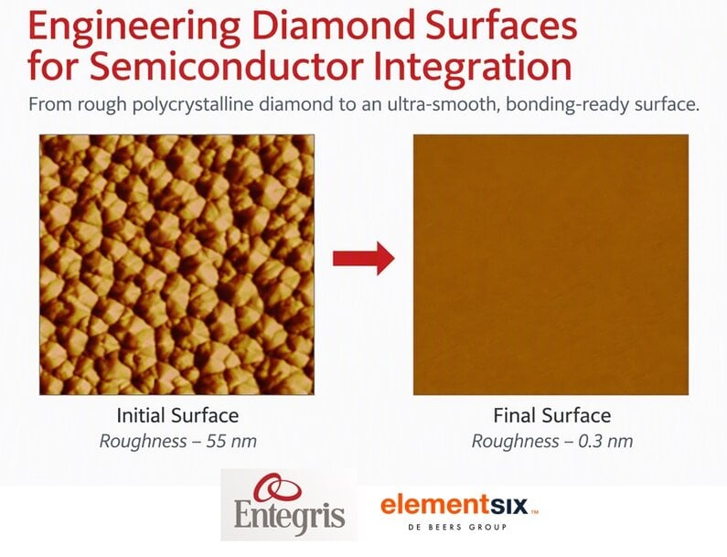
Element Six (E6) and Entegris have announced a strategic collaboration to accelerate the integration of synthetic diamond into advanced semiconductor packaging. As artificial intelligence (AI) and high-performance computing (HPC) drive exponential increases in chip power density, conventional thermal management technologies are rapidly approaching their practical limits. To address these critical bottlenecks in next-generation graphics processing units (GPUs) and radio frequency (RF) devices, the partnership aims to leverage synthetic diamond—which boasts the highest room-temperature thermal conductivity of any known material—to improve device efficiency, performance, and scalability for data centers and telecommunications infrastructure.
Overcoming integration barriers with surface engineering
While synthetic diamond possesses exceptional thermal properties, its widespread adoption has historically been hindered by the complexities of bonding it to semiconductor wafers without introducing high thermal boundary resistance at the interface. The collaboration merges E6’s deep expertise in engineering both polycrystalline and single-crystal synthetic diamond with Entegris’ leadership in semiconductor surface engineering and materials science. Together, they are developing cost-effective, scalable approaches for wafer-level heterogeneous integration. By providing a broad portfolio of customized engineered surfaces and advanced bonded diamond technologies, the partners will enable semiconductor manufacturers to seamlessly incorporate diamond cooling solutions into diverse device architectures without compounding manufacturing complexity.
Additional Context: Thermal boundary resistance and CVD diamond synthesis
This section details semiconductor thermal physics and synthetic diamond manufacturing principles not included in the original press release.
In advanced 2.5D and 3D heterogeneous packaging (such as TSMC's CoWoS), multiple high-power logic and memory dies are stacked tightly together, creating severe localized "hot spots" with massive heat flux. While synthetic diamond—typically grown via Chemical Vapor Deposition (CVD) using a microwave plasma to deposit carbon atoms layer by layer—offers a thermal conductivity of up to 2,200 W/(m·K) (more than five times that of copper), simply placing it next to a silicon die is insufficient. The bottleneck lies in the microscopic interface between the dissimilar materials. This phenomenon, known as Thermal Boundary Resistance (or Kapitza resistance), occurs because phonons (the quantum mechanical vibrations responsible for heat transfer in non-metals) scatter when crossing the boundary between the silicon lattice and the diamond lattice. Advanced surface engineering focuses on atomic-level bonding techniques—such as ultra-thin transition adhesion layers or direct hydrophilic wafer bonding—to acoustically match these lattices. This minimizes phonon scattering at the interface, allowing heat to pass through efficiently and unlocking the diamond's true heat-spreading potential.
Edited by an industrial journalist, Lekshman Ramdas, with AI assistance.
www.e6.com
